


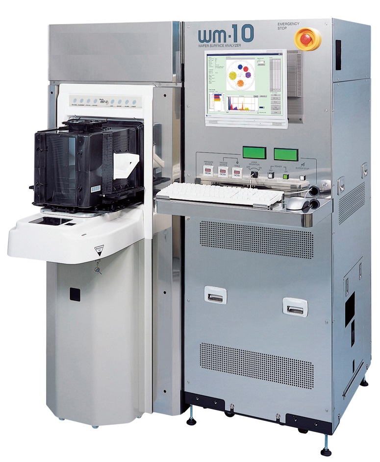
TAKANO_WM-10
UPLUS ENGINEERINGSemicon Wafer Surface Inspection system WM-10
More sensitivity and Eco-friendly Ever seen under 90nm process node
WM-10 is high-end surface inspection system of our WM Series. This product can detect any type of micro defects on non-patterned wafer of semiconductor device and avilable for wide-range wafer size from 6-inch to 8-inch or from 8-inch to 12-inch. And this product is equipped with bule-violet semiconductor laser which is the world's first wafer surface analyzer in this field. This laser makes a contribution to reduce the running cost. This prduct is eco-friendly, as well as being of high quality high speed measuring and low-priced.
Features
- Provied the best solution for 65-90nm process node
- World's first wafer surface analyzer using the violet-LD
- Drastic reduction of the running cost by using the violet-LD
- Low price / High performance / Small foot print / Easy operation
- Separability of COP's and real dusts by using original optical system
Specification
| Light Source | Violet LD(blue-violet semiconductor) |
|---|---|
| Scan system | Helical Scan |
| Sensitivity | 48nm *Bare Wafer |
| Repeatability | o/X ≤ 1% *99% or more |
| Supported Wafer | Bare Wafer / Coated Wafer |
| Wafer Size | 12/8 inch or 8/6 inch |
| Dimension Size WXDXH | 1.482 X 1,173 X 1,950mm |
| Weight | 900kg |
Option
- Automatic sensitivity adjustment function Haze function
- Double wafer port
- Map overlapping function
- X-Y coordinate output (Communication software)
- Host communication software