


TAKANO_WM-10
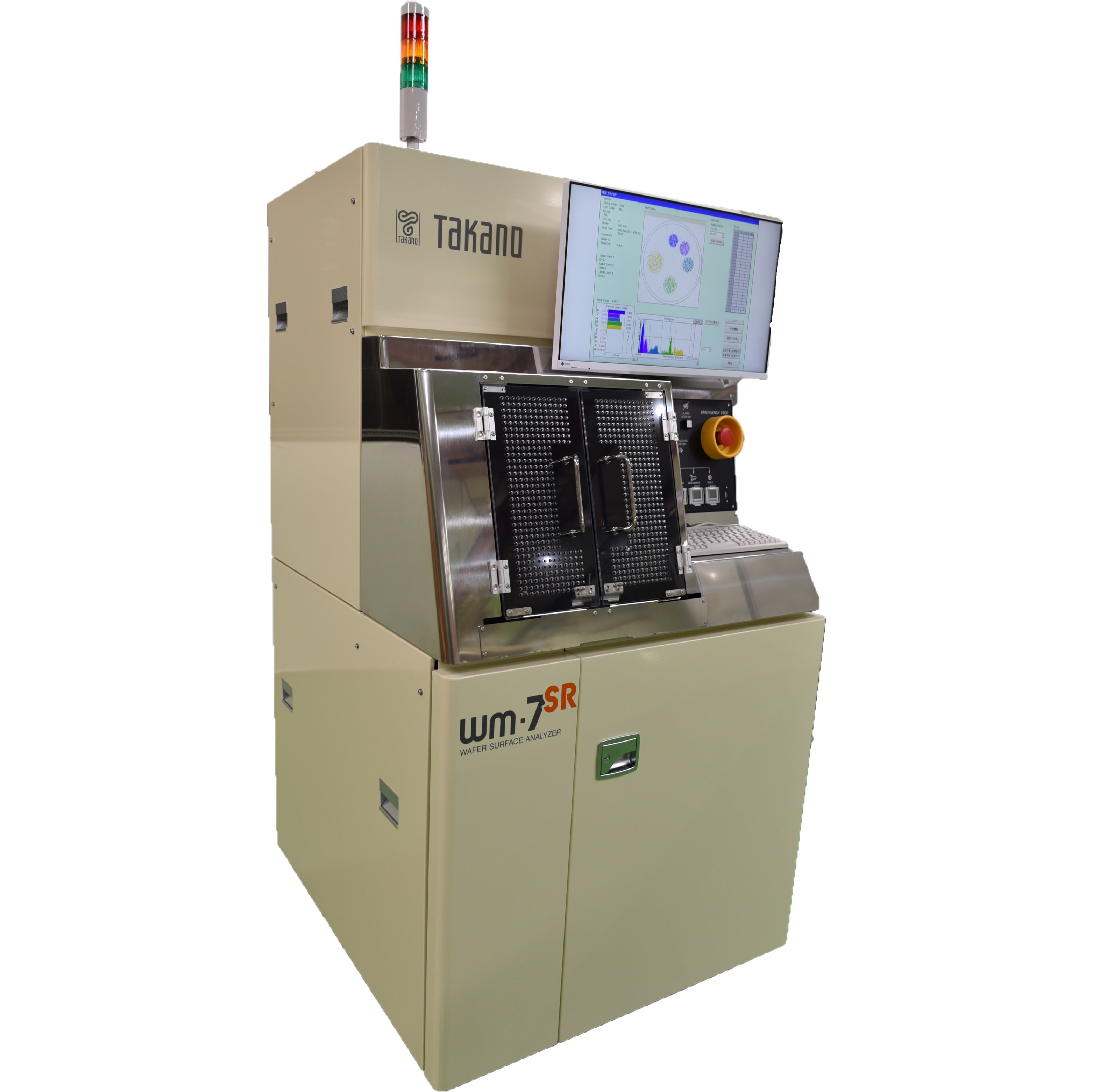
UPLUS ENGINEERINGSemicon Wafer Surface Inspection system WM-7SR
Available for non pattern wafer by new optical system.
WM-7SR has been added to our product line up of wafer surface analyzer, to respond to the growing demand of the silicon wafer. TAKANO's original optical system improved WM-7SR makes an achievement to measure with highly accurate measurement for silicon wafer. This model would be great for R&D department, test production, and small scale manufacturing line. WM-7SR is also equipped with the bule-violet semiconductor laser as WM-7. The bule-violet semiconductor laser makes a contribution to reduce the running cost of the factory.
Features
- Available for a clear wafer material
- World's first wafer surface analyzer using the violet-LD
- Drastic reduction of the running cost by using the violet-LD
- Low price / High performance / Small foot print / Easy operation
- Available from 2-inch to 8-inch
- Variety of options
Specification
| Light Source | Violet LD(blue-violet semiconductor) |
|---|---|
| Scan system | Helical Scan |
| Sensitivity | 80nm *Bare Wafer |
| Repeatability | σn/x≦1% *99% or more |
| Supported Wafer | Bare wafer / Coated Wafer |
| Wafer Size | 2inch~8inch |
| Dimension Size WxDxH | 800 X 900 X 1,650mm |
| Weight | 600kg |
Option
- Automatic sensitivity adjustment function Haze function
- Double wafer port
- Map overlapping function
- X-Y coordinate output (Communication software)
- Host communication software